Alle Kategorien
-
Integrierte schaltkreise (ICS)
Integrierte schaltkreise (ICS)
- Schnittstelle - Sensor, kapazitive Berührung(642)
- Spezialisierte ICS(12302)
- PMIC-Spannungsregler-besonderer Zweck(5644)
- PMIC-Spannungsregler-lineare Regler(793)
- PMIC-Spannungsregler-linear + Switching(1829)
- PMIC-Spannungsregler-linear(70981)
- PMIC-Spannungsregler-DC DC Switching Regulators(39569)
- PMIC-Regler-DC-DC-Switching-Controller(13507)
- PMIC-Spannungs-Referenz(9453)
- PMIC-v/f und f/v-Wandler(145)
- PMIC-Thermal Management(592)
- PMIC-Supervisor(47946)
- PMIC-RMS bis DC-Wandler(170)
- PMIC-Netzteil-Controller, Monitore(2104)
- PMIC-Power over Ethernet (PoE) Controller(1008)
- PMIC-Power Management-spezialisierte(7722)
- PMIC-Netzschalter, Treiber laden(7706)
- PMIC-PFC (Power Factor Correction)(1222)
- PMIC oder Steuerungen, ideale Dioden(705)
- PMIC-Motor-Treiber, Regler(4712)
- PMIC-Beleuchtung, Ballast-Regler(560)
- PMIC-LED-Treiber(7282)
- PMIC-Laser-Treiber(573)
- PMIC-Hot-Swap-Controller(2816)
- PMIC-Gate-Treiber(7083)
- PMIC-voll, Half-Bridge-Treiber(1342)
- PMIC-Energy Messung(654)
- PMIC-Display-Treiber(1435)
- PMIC-derzeitige Regulierung/Management(1481)
- PMIC-Batterie-Management(5553)
- PMIC-Ladegeräte(3831)
- PMIC-AC DC Konverter, Offline Schalter(4905)
- Memory-Controller(358)
- Memory-Konfigurations-Proms für FPGAs(639)
- Speicher-Akkus(13)
- Erinnerung(65694)
- Logic-universelle Bus-Funktionen(706)
- Logic-Übersetzer, Level-Shifter(2854)
- Logik-Specialty Logic(1870)
- Logik-Signal-Schalter, Multiplexer, Decoder(9420)
- Logic-Shift-Register(2665)
- Logic-Parity Generatoren und Checkers(335)
- Logic-multivibratoren(831)
- Logik-Latches(3658)
- Logik - Tore und Wechselrichter - Multifunktion, konfigurierbar(1687)
- Logik-Tore und Wechselrichter(16453)
- Logic-Flip Flops(7780)
- Logik-FIFOs Speicher(4240)
- Logik-Zähler, Trennlinien(3456)
- Logik-Vergleichsoperator(592)
- Logik-Puffer, Treiber, Receiver, Transceiver(17835)
- Linear-Video-Verarbeitung(2909)
- Linear-Vergleichsoperator(5084)
- Linear-analoge Multiplikatoren, Trennwände(263)
- Linear-Verstärker-Video Amps und Module(1905)
- Linear-Verstärker-Spezial-Zweck(1856)
- Linear - Verstärker - Instrumentierung, OP -Verstärker, Pufferverstärker(34236)
- Linear-Verstärker-Audio(4567)
- Interface-Voice Record und Playback(556)
- Schnittstelle - UARTs (Universal Asynchronous Receivers -Sender)(1237)
- Schnittstelle-Telecom(4467)
- Interface-spezialisierte(4833)
- Interface-Signal Terminatoren(333)
- Interface-Signal-Puffer, Repeater, Splitter(1449)
- Interface-Serializer, Deserializer(1480)
- Schnittstellen-Sensor und Detektor-Interfaces(1524)
- Interface-Module(169)
- Interface-Modems-ICS und Module(407)
- Interface-e/a-Expander(1136)
- Interface-Filter-aktiv(1226)
- Interface-Encoder, Decoder, Konverter(714)
- Interface-Treiber, Receiver, Transceiver(20755)
- Interface-Direct Digital Synthesis (DDS)(117)
- Interface-Controller(3628)
- Interface-Codecs(1676)
- Schnittstelle - Analoge Switches, Multiplexer, Demultiplexer(12567)
- Schnittstelle-analoge Schalter-spezieller Zweck(2533)
- Embedded-System on Chip (SoC)(4496)
- Embedded-PLDs (programmierbare Logik-Vorrichtung)(971)
- Embedded-Mikroprozessoren(10083)
- Embedded-Mikrocontroller-anwendungsspezifische(2275)
- Embedded-Mikrocontroller(99285)
- Eingebettet - Mikrocontroller, Mikroprozessor, FPGA -Module(1527)
- Eingebettet - FPGAs (Feldprogrammiergate -Array) mit Mikrocontrollern(81)
- Embedded-FPGAs (Field Programmable Gate Array)(27747)
- Embedded-DSP (Digital Signal Processors)(4081)
- Eingebettet - CPLDs (komplexe programmierbare Logikgeräte)(5187)
- Datenerfassung-Touch Screen Controller(1210)
- Datenerfassung-Digital to Analog Converter (DAC)(14419)
- Datenerfassung-digitale Potentiometer(6250)
- Datenerfassung-analog zu Digital Converters (ADC)(17776)
- Datenerfassung-analoges Frontend (AFE)(787)
- Datenerfassung-MDE/DACs-spezieller Zweck(3043)
- Clock/Timing-Uhren in Echtzeit(2446)
- Uhr/Timing - programmierbare Timer und Oszillatoren(23469)
- Clock/Timing-IC-Akkus(4)
- Takt/Timing-Delay Lines(1049)
- Uhr/Timing - Uhrengeneratoren, PLLS, Frequenzsynthesizer(32775)
- Clock/Timing-Clock Puffer, Treiber(4568)
- Clock/Timing-anwendungsspezifische(8652)
- Audio Spezial-Zweck(1564)
Relevanter Hersteller


-
Diskrete Halbleiter-Produkte
Diskrete Halbleiter-Produkte
- Aktuelle Regulierung - Dioden, Transistoren(1090)
- Transistoren-besonderer Zweck(226)
- Transistoren-programmierbare Unijunction(48)
- Transistoren-jfets(1558)
- Transistoren-IGBTs-Einzel(4799)
- Transistoren-IGBTs-Module(63420)
- Transistoren-IGBTs-Arrays(26)
- Transistoren-FETs, MOSFETs-Einzel(48330)
- Transistoren-FETs, MOSFETs-RF(4903)
- Transistoren-FETs, MOSFETs-Arrays(6641)
- Transistoren-Bipolar (BJT)-einzeln, Pre-biased(4539)
- Transistoren-Bipolar (BJT)-Einzel(25800)
- Transistoren-Bipolar (BJT)-RF(2087)
- Transistoren-bipolare (BJT)-Arrays, Pre-biased(2115)
- Transistoren-bipolare (BJT)-Arrays(2310)
- Thyristor-triacs(4044)
- Thyristoren-SCRs-Module(3967)
- Thyristoren-SCRs(5436)
- Thyristoren-diacs, sidacs(319)
- Power Driver Module(1627)
- Dioden-zenerdioden-Einzel(87483)
- Dioden-zenerdioden-Arrays(2619)
- Dioden - variable Kapazität (Varik, Varaktoren)(1200)
- Dioden-RF(2753)
- Dioden-Gleichrichter-Einzel(67528)
- Dioden-Gleichrichter-Arrays(20581)
- Dioden-Brücke-Gleichrichter(11700)
Relevanter Hersteller


-
RF/if und RFID
RF/if und RFID
- SIM -Karten für Abonnenten -Identifikationsmodul (SIM)(77)
- RF -Zirkulatoren und Isolatoren(1742)
- RFID, RF-Zugang, Monitoring-ICS(1550)
- RFID Transponder, Tags(747)
- RFID Lesegeräte(464)
- RFID -Bewertungs- und Entwicklungskits, Boards(30)
- RFID Antennen(329)
- RFI und EMI - Abschirm- und Absorbungsmaterialien(6444)
- HF und EMI-Kontakte, Fingerstock und Dichtungen(7497)
- RF Transmitter(668)
- RF Transceiver Module(6900)
- RF-Transceiver ICS(4169)
- HF-Schalter(9276)
- RF Shields(16401)
- HF-Receiver(1998)
- HF -Empfänger, Sender und Transceiver -Einheiten(2763)
- RF Power Divider/Splitter(1223)
- RF Power Controller ICs(86)
- HF-Modulatoren(710)
- HF-Mixer(2800)
- RF misc ICS und Module(3276)
- HF-Front-End (LNA + PA)(419)
- RF -Bewertungs- und Entwicklungskits, Boards(747)
- HF-gerichtete Kupplung(2718)
- RF Diplexer(1464)
- RF-Detektoren(412)
- RF-Demodulatoren(249)
- HF-Antennen(12319)
- HF-Verstärker(19651)
- Balun(1496)
- Dämpfungsglieder(4852)
Relevanter Hersteller


-
Optoelektronik
Optoelektronik
- Optomechanisch(480)
- Leuchten(125)
- Laserdioden, Lasermodule - Laserlieferung, Laserfasern(345)
- Hene Lasersysteme(31)
- Hene Laserköpfe(27)
- Hintergrundbeleuchtung anzeigen(93)
- Xenon-Beleuchtung(387)
- Touchscreen-Overlays(453)
- Panel Indicators, Pilot Lights(75729)
- Optik-Remote-Phosphor-Lichtquelle(269)
- Optik-Reflektoren(665)
- Optik-leichte Rohre(5384)
- Optik-Objektive(4951)
- LEDs-Spacer, Unentschieden(2718)
- LEDs-Lamp-Ersetzungen(29718)
- LEDs - Leiterplattenindikatoren, Arrays, Lichtstäbe, Balkendiagramme(9083)
- LED-thermische Produkte(667)
- LED-Beleuchtung(64)
- LED-Beleuchtung-weiß(37580)
- LED-Beleuchtung-Farbe(4728)
- LED-Beleuchtung-Maiskolben, Motoren, Module(28735)
- LED-Anzeige-diskret(27601)
- Laserdioden, Module(1553)
- Lampen-Glühlampen, Neons(311004)
- Lampen-Kälte-Fluoreszenz (KKL) & UV(164)
- Wechselrichter(7728)
- Infrarot, UV, sichtbare Strahler(3871)
- Fiber Optics-Transmitter-Antrieb integriert(4085)
- Fiber Optics-Transmitter-diskrete(350)
- Fiber Optics-Transceiver Module(18758)
- Fiberoptik-Switches, Multiplexer, Demultiplexer(1387)
- Fiberoptik-Receiver(695)
- Fiberoptik-Dämpfung(654)
- Elektrolumineszenz(102)
- Display, Monitor-Interface Controller(98)
- Display-Module-Vakuum-Leuchtstofflampen (VFD)(249)
- Module anzeigen-LED Dot Matrix und Cluster(865)
- Display-Module-LED-Zeichen und numerische(5421)
- Display-Module-LCD, OLED, Graphic(4654)
- Display-Module-LCD, OLED-Zeichen und numerische(2202)
- Display-Blenden, Objektive(88)
- Adresse, Spezialität(458)
Relevanter Hersteller


-
Sensoren, Wandler
Sensoren, Wandler
- Ultraschallempfänger, Sender - Industrial(115)
- Temperatursensoren - Thermostate - Mechanisch - Industrielles(3103)
- Temperatursensoren - Analog und digitaler Ausgang - Industrial(209)
- Näherungssensoren - Industrial(13611)
- Drucksensoren, Wandler - Industrie(26503)
- Optische Sensoren - Photonik - Zähler, Detektoren, SPCM (Einzelphotonzählmodul)(751)
- Optische Sensoren - Kameramodule(875)
- Magnetsensoren - Position, Nähe, Geschwindigkeit (Module) - Industrie(554)
- Kraftsensoren - Industrial(346)
- Flusssensoren - Industrielles(151)
- Float, Level Sensoren - Industrial(310)
- Encoder - Industrial(4980)
- Farbsensoren - Industrial(50)
- Berührungssensoren(100)
- Ultraschall-Receiver, Transmitter(2421)
- Temperatursensoren-Thermostat-Solid State(1096)
- Temperatursensoren-Thermostate-mechanisch(3397)
- Temperatursensoren - Thermoelemente, Temperatursonden(1921)
- Temperatursensoren - RTD (Widerstandstemperaturdetektor)(1525)
- Temperatursensoren-PTC-Thermistoren(2273)
- Temperatursensoren-ntc-thermistoren(13259)
- Temperatursensoren-Analog und Digital Output(3928)
- DMS(1399)
- Spezialisierte Sensoren(1861)
- Solarzellen(503)
- Schock-Sensoren(84)
- Sensor-Interface-Junction-Blöcke(2519)
- Sensor-Kabel-Baugruppen(22011)
- Proximity/Belegung Sensoren-fertige Einheiten(725)
- Näherungsschalter(2860)
- Drucksensoren, Wandler(11317)
- Positionssensoren - Winkel, lineare Positionsmessung(6022)
- Optische Sensoren-reflektierende-Logik-Ausgang(194)
- Optische Sensoren - reflektierend - analoge Ausgang(432)
- Optische Sensoren-Phototransistoren(1027)
- Optische Sensoren - Photointerrupter - Schlitztyp - Transistorausgang(1427)
- Optische Sensoren - Photointerrupter - Schlitztyp - Logikausgabe(1215)
- Optische Sensoren-Lichtschranke, Industrial(16763)
- Optische Sensoren-Photodioden(1543)
- Optische Sensoren-Foto-Detektoren-Remote Receiver(2605)
- Optische Sensoren-Foto-Detektoren-Logik-Ausgang(146)
- Optische Sensoren-Foto-Detektoren-CDs-Zellen(74)
- Optische Sensoren-Distanz-Messung(377)
- Optische Sensoren-Ambient Light, IR, UV Sensoren(1305)
- Multifunktions(558)
- Motion Sensors-Vibration(337)
- Motion Sensors-Tilt Schalter(67)
- Bewegungsmelder-optisch(719)
- Motion Sensors-Neigungssensoren(175)
- Motion Sensors-Imus (Trägheit-Maßeinheiten)(416)
- Motion Sensors-Kreisel(214)
- Motion Sensors-Beschleunigungsmesser(1911)
- Magnete-Sensor abgestimmt(119)
- Magnete-Multi Purpose(1965)
- Magnetische Sensoren-Schalter (Solid State)(3700)
- Magnetsensoren - Position, Nähe, Geschwindigkeit (Module)(5199)
- Magnetische Sensoren-linear, Kompass (ICS)(1247)
- Magnetsensoren - Kompass, Magnetfeld (Module)(35)
- LVDT -Wandler (linearer variabler Differentialtransformator)(204)
- IrDA Transceiver-Module(196)
- Bildsensor, Kamera(2235)
- Feuchtigkeit-Sensoren(1425)
- Gas-Sensoren(1217)
- Force Sensoren(188)
- Durchfluss-Sensoren(550)
- Float, Level Sensoren(1343)
- Encoder(6357)
- Staub-Sensoren(43)
- Aktuelle Wandler(3455)
- Color Sensoren(85)
- Verstärker(1905)
Relevanter Hersteller


-
Anschlüsse, Verbindungen
Anschlüsse, Verbindungen
- USB, DVI, HDMI -Stecker(446)
- Festkörperbeleuchtungsstecker(555)
- Steckdosen für ICs, Transistoren(953)
- Steckbare Steckverbinder(1221)
- Photovoltaik (Solarpanel) Anschlüsse(136)
- Glasfaseranschlüsse(370)
- FFC, FPC (flache flexible) Anschlüsse(761)
- D-Sub, D-förmige Stecker(2887)
- Koaxialverbinder (RF)(2389)
- Rundanschlüsse(14162)
- Stromanbeter Blade Type(273)
- Stecker und Behälter(2597)
- USB, DVI, HDMI Stecker-Adapter(572)
- USB, DVI, HDMI -Stecker(4298)
- Klemmen-Wire to Board Steckverbinder(217)
- Klemmen-Draht-Steckverbinder(4322)
- Klemmen-Draht-Pin Stecker(328)
- Terminals-Revolver Steckverbinder(1273)
- Terminals-spezialisierte Steckverbinder(2042)
- Klemmen-Spaten Verbinder(3902)
- Klemmen-Löten/Stecker(345)
- Klemmen-Verschraubungen(745)
- Klemmen-Ring Steckverbinder(12596)
- Klemmen-rechteckige Steckverbinder(4747)
- Terminals - Schnellverbindungen, schnelle Trennungsanschlüsse(8514)
- Klemmen-PC PIN, Single Post Connectors(3776)
- Klemmen-PC-Pin-Buchsen, Sockel-Steckverbinder(5883)
- Klemmen-magnetische Draht-Steckverbinder(1653)
- Klemmen-Messer Steckverbinder(112)
- Klemmen-Gehäuse, Stiefel(2850)
- Klemmen-Folie Steckverbinder(108)
- Klemmen-Barrel, Bullet-Steckverbinder(1107)
- Klemmen-Adapter(137)
- Terminal-Streifen und Revolver-Boards(1159)
- Terminal Junction Systeme(2533)
- Anschlussblöcke-Draht an Bord(43615)
- Terminal Blocks-spezialisierte(3722)
- Terminal Blocks-Power Distribution(847)
- Anschlussblöcke-Panel Mount(1359)
- Terminal Blocks-Interface Module(1819)
- Anschlussblöcke-Kopfzeilen, Stecker und Buchsen(119920)
- Anschlussblöcke-DIN-Schiene, Kanal(9373)
- Anschlussblöcke-Kontakte(65)
- Anschlussblöcke-Barrier Blocks(47517)
- Anschlussblöcke-Adapter(1059)
- Solid State Lighting Verbinder-Kontakte(271)
- Festkörperbeleuchtungsstecker(1344)
- Buchsen für ICS, Transistoren-Adapter(275)
- Steckdosen für ICs, Transistoren(22148)
- Shunts, Jumper(907)
- Rechteckige Verbinder-Feder geladen(7721)
- Rechteckige Steckverbinder-Gehäuse(43023)
- Rechteckige Verbinder-Kopfzeilen, Spezial-PIN(6129)
- Rechteckige Anschlüsse - Header, Gefäße, weibliche Sockel(229601)
- Rechteckige Verbinder-Kopfzeilen, männliche Pins(543338)
- Rechteckige Anschlüsse - kostenloses Hängen, Panelhalterung(30142)
- Rechteckige Verbinder-Kontakte(10681)
- Rechteckige Anschlüsse - Board in, Direktdraht zum Board(2432)
- Rechteckige Verbinder-Adapter(475)
- Rechteckig - Brett zu Board -Steckern - Header, Behälter, weibliche Sockel(9)
- Rechteckig - Brett zu Board -Steckern - Header, männliche Stifte(2)
- Rechteckige Anschlüsse - Board -Abstandshalter, Stacker (Board zu Board)(238901)
- Rechteckige Anschlüsse - Arrays, Kantentyp, Mezzanin (Board zu Board)(37853)
- Stromanschluss-Eingänge, Steckdosen, Module(10310)
- Steckbare Steckverbinder(6049)
- Photovoltaik- (Solarpanel) Anschlüsse - Kontakte(77)
- Photovoltaik (Solarpanel) Anschlüsse(504)
- Modulare Steckverbinder-Verdrahtung Blöcke(99)
- Modulare Steckverbinder-Stecker(1674)
- Modulare Steckverbinder-Stecker Gehäuse(181)
- Modulare Steckverbinder-Buchsen mit magnetischen(10152)
- Modulare Steckverbinder-Buchsen(23416)
- Modulare Steckverbinder-Adapter(855)
- Memory Connectors-PC Cards-Adapter(21)
- Memory Connectors-PC Card Sockets(3299)
- Memory Connectors-Inline Modul Sockets(3390)
- LGH Steckverbinder(764)
- Keystone-Einsätze(2758)
- Keystone-Frontplatte, Frames(1926)
- Heavy Duty Steckverbinder-Einsätze, Module(4190)
- Schwerlastanschlüsse - Gehäuse, Kapuzen, Basen(17226)
- Heavy Duty Steckverbinder-Frames(523)
- Heavy Duty Steckverbinder-Kontakte(1832)
- Heavy Duty Steckverbinder-Baugruppen(671)
- LWL-Steckverbinder-Gehäuse(919)
- Glasfaser-Steckverbinder - Adapter(4455)
- LWL-Steckverbinder(3001)
- FFC, FPC (flache flexible) Steckverbinder - Gehäuse(652)
- FFC, FPC (flache flexible) Anschlüsse - Kontakte(202)
- FFC, FPC (flache flexible) Anschlüsse(18691)
- D-Sub, d-förmige Steckverbinder-Terminatoren(47)
- D-Sub, d-förmige Steckverbinder-Gehäuse(12238)
- D-Sub, d-förmige Steckverbinder-Kontakte(2714)
- D-Sub, D-förmige Steckverbinder-Rückenschalen, Kapuzen(5995)
- D-Sub, d-förmige Steckverbinder-Adapter(1304)
- D-Sub Steckverbinder(141346)
- D-förmige Steckverbinder-Centronics(8770)
- Kontakte, Frühling geladen und Druck(630)
- Kontakte-Multi Purpose(6196)
- Kontakte-"Leadframe"(122)
- Koaxial-Steckverbinder (RF)-Terminatoren(1231)
- Koaxial-Steckverbinder (RF)-Kontakte(480)
- Koaxial-Steckverbinder (RF)-Adapter(6386)
- Koaxialverbinder (RF)(25734)
- Rundsteckverbinder-Gehäuse(441226)
- Rundsteckverbinder-Kontakte(4737)
- Rundsteckverbinder-backschalen und Kabel-Klemmen(53692)
- Rundsteckverbinder-Adapter(8839)
- Rundanschlüsse(1196254)
- Card Edge Steckverbinder-Gehäuse(469)
- Karte Edge Verbinder-edgeboard Verbinder(672683)
- Card Edge Verbinder-Kontakte(325)
- Card Edge Verbinder-Adapter(73)
- Blade Type Power Steckverbinder-Gehäuse(837)
- Blade Type Power Connectors-Kontakte(393)
- Stromanbeter Blade Type(4163)
- Zwischen Serien-Adapter(649)
- Barrel-Stromanschluss(935)
- Barrel-Audio-Anschlüsse(2432)
- Barrel-Audio Adapter(92)
- Banana und Tip Steckverbinder-Buchsen, Stecker(1644)
- Banana and Tip Connectors-Binding Posts(239)
- Banana und Tip Steckverbinder-Adapter(75)
- Backplane Steckverbinder-spezialisiert(45586)
- Backplane Steckverbinder-Gehäuse(6863)
- Backplane Steckverbinder-Hard metrisch, Standard(6297)
- Backplane Steckverbinder-DIN 41612(9408)
- Backplane Steckverbinder-Kontakte(3583)
- Backplane Connectors-ARINC Einsätze(2357)
- Backplane Steckverbinder-ARINC(3789)
Relevanter Hersteller


-
Widerstände
-
Kondensatoren
Kondensatoren
- Aluminium-Elektrolytkondensatoren(16817)
- Trimmer, Variable Kondensatoren(3151)
- Dünne Folien-Kondensatoren(3473)
- Tantal-Kondensatoren(136103)
- Tantal-Polymer-Kondensatoren(9778)
- Silizium-Kondensatoren(320)
- Niob Oxide Kondensatoren(330)
- Mica und PTFE Kondensatoren(9101)
- Folien-Kondensatoren(150406)
- Elektrische Doppelschichtkondensatoren (EDLC), Superkondensatoren(2782)
- Keramische Kondensatoren(833829)
- Kondensatoren-Netzwerke, Arrays(2383)
- Aluminium-Elektrolytkondensatoren(125325)
- Aluminium-Polymer-Kondensatoren(7544)
Relevanter Hersteller


-
Transformatoren
Transformatoren
Relevanter Hersteller


-
Isolatoren
-
Kristalle, Oszillatoren, Resonatoren
Kristalle, Oszillatoren, Resonatoren
Relevanter Hersteller


-
Switches
Switches
- Verriegelungsschalter(2893)
- Emergency-Stop-Schalter (E-Stop)(1160)
- Kabelzugschalter(571)
- Toggle-Schalter(33608)
- Rändelrads Schalter(742)
- Schalter(14263)
- Snap-Aktion, Endschalter begrenzen(28077)
- Slide-Schalter(5166)
- Selector-Schalter(9720)
- Rotary Switches(13850)
- Rocker Schalter(53790)
- Drucktaste-Schalter-Hall-Effekt(127)
- Drucktaste Schalter(190826)
- Programmierbare Display-Switches(39)
- Navigations-Schalter, Joystick(1882)
- Magnetische, Reed-Schalter(1399)
- Keypad-Schalter(637)
- Keylock Schalter(3684)
- DIP Schalter(7747)
- Konfigurierbare Switch-Komponenten-Objektiv(1435)
- Konfigurierbare Schalter-Komponenten-Lichtquelle(1236)
- Konfigurierbare Switch-Komponenten-Contact Block(1401)
- Konfigurierbare Switch-Komponenten-Body(16077)
- Disconnect-Switch-Komponenten(2567)
Relevanter Hersteller


-
Relais
Relais
- Sicherheitsrelais(1310)
- Reedrelais(1735)
- Hochfrequenz (RF) -Relais(1190)
- Schütze (Festkörper)(686)
- Schütze (elektromechanisch)(11952)
- Kfz-Relais(1881)
- Solid State Relais(10652)
- Signal-Relais, bis zu 2 Ampere(9149)
- Relay-Sockets(2075)
- Power Relays, über 2 Ampere(31604)
- E / A-Relaismodule(712)
- I/o-Relay-Module-Input(2)
- I/o-Relay-Modul-Racks(247)
Relevanter Hersteller


Sprache auswählen
Aktuelle Sprache
Deutsch
- English
- Deutsch
- Italia
- Français
- 日本語
- 한국의
- русский
- Svenska
- Nederland
- español
- Português
- polski
- Suomi
- Gaeilge
- Slovenská
- Slovenija
- Čeština
- Melayu
- Magyarország
- Hrvatska
- Dansk
- românesc
- Indonesia
- Ελλάδα
- Български език
- Afrikaans
- IsiXhosa
- isiZulu
- lietuvių
- Maori
- Kongeriket
- Монголулс
- O'zbek
- Tiếng Việt
- हिंदी
- اردو
- Kurdî
- Català
- Bosna
- Euskera
- العربية
- فارسی
- Corsa
- Chicheŵa
- עִבְרִית
- Latviešu
- Hausa
- Беларусь
- አማርኛ
- Republika e Shqipërisë
- Eesti Vabariik
- íslenska
- မြန်မာ
- Македонски
- Lëtzebuergesch
- საქართველო
- Cambodia
- Pilipino
- Azərbaycan
- ພາສາລາວ
- বাংলা ভাষার
- پښتو
- malaɡasʲ
- Кыргыз тили
- Ayiti
- Қазақша
- Samoa
- සිංහල
- ภาษาไทย
- Україна
- Kiswahili
- Cрпски
- Galego
- नेपाली
- Sesotho
- Тоҷикӣ
- Türk dili
- ગુજરાતી
- ಕನ್ನಡkannaḍa
- मराठी
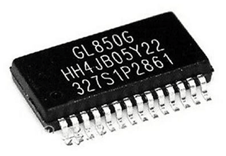
Understanding GL850G USB Hub Controller & Its Internal Architecture
Zeit: 2026/05/19
Durchsuchen: 63
USB ports are still important in many electronic devices, especially when one connection needs to support several USB peripherals at the same time. The GL850G USB 2.0 Hub Controller helps expand one USB connection into multiple downstream USB ports while managing data transfer, power control, port detection, and device communication inside the hub. This article explains the GL850G, including its main features, internal working structure, pinout, typical application circuit, and more.
Catalog
What is GL850G USB 2.0 Hub Controller?
The GL850G USB 2.0 Hub Controller is a hub controller IC from Genesys Logic designed to expand one USB connection into multiple USB ports. It fully complies with the USB 2.0 specification and supports high-speed data transfer up to 480 Mbps.
The GL850G includes an embedded 8-bit RISC processor, built-in voltage regulators, power management support, status LED control, and EEPROM configuration for custom VID/PID settings. It also supports bus-powered and self-powered designs, giving system designers more flexibility. As a single TT hub controller, the GL850G offers a cost-effective solution for USB 2.0 hub designs while maintaining stable communication between the upstream host and downstream ports.
If you are interested in purchasing the GL850G, feel free to contact us for pricing and availability.
GL850G Main Features and Specifications
USB 2.0 Compliance and Data Transfer Support
The GL850G is fully compliant with USB Specification Revision 2.0, which means it can operate as a standard USB 2.0 hub controller. Its upstream port supports both high-speed and full-speed traffic, allowing it to communicate properly with the host system. The downstream ports support high-speed, full-speed, and low-speed USB devices, so different USB peripherals can connect through the same hub controller. It is also backward compatible with USB 1.1, making it suitable for older USB devices.
USB Communication Pipes
The GL850G includes one control pipe and one interrupt pipe for USB communication. The control pipe uses endpoint 0 with a 64-byte data payload and is mainly used for device setup, enumeration, and standard USB control requests. The interrupt pipe uses endpoint 1 with a 1-byte data payload and helps report hub status changes, such as device connection, disconnection, or port condition updates.
On-Chip 8-Bit Microprocessor
The GL850G has an on-chip 8-bit microprocessor that manages hub control functions internally. This processor uses a RISC-like architecture and a USB-optimized instruction set, allowing the chip to handle USB hub tasks efficiently. It operates at 6 MIPS at 12 MHz and includes 64-byte RAM and 4K mask ROM, which store and execute the basic control functions needed for hub operation.
Custom VID/PID and Port Configuration Support
The GL850G supports customized VID and PID settings through an external EEPROM or SMBUS. This allows manufacturers to assign their own vendor ID and product ID instead of using default settings. The downstream port configuration can also be programmed through EEPROM or SMBUS, giving designers more control over how many ports are enabled and how the hub appears to the host system.
Single Transaction Translator Architecture
The GL850G uses a Single Transaction Translator, or STT, architecture. This means one transaction translator is shared by all downstream ports when handling full-speed or low-speed devices connected to a high-speed USB 2.0 host. This design helps reduce cost and simplifies the hub controller, but performance may be more limited when several slower USB devices are active at the same time.
Integrated USB 2.0 Transceiver
The GL850G includes an integrated USB 2.0 transceiver, which handles the physical USB signaling between the hub controller, the host, and connected devices. This reduces the need for extra external components and helps simplify board-level design. The built-in transceiver supports stable signal communication for USB 2.0 hub operation.
EMI Reduction and ESD Recovery Support
The GL850G improves output drivers with slew-rate control to help reduce EMI, or electromagnetic interference. This is important because USB signal lines can generate noise if signal edges are too sharp or poorly controlled. The chip also includes internal power-fail detection for ESD recovery, helping the controller recover more safely after electrostatic discharge or power-related disturbances.
Low BOM Cost and Built-In Voltage Regulation
The GL850G is designed to reduce total board cost by integrating several required functions inside the chip. It includes a built-in 5V to 3.3V regulator, which reduces the need for an external 3.3V regulator in many designs. This helps lower BOM cost, saves PCB space, and makes the hub circuit easier to implement.
Built-In USB Pull-Up and Pull-Down Resistors
The GL850G includes a built-in upstream 1.5KΩ pull-up resistor and downstream 15KΩ pull-down resistors. These resistors are required for proper USB device detection and bus state control. By integrating them inside the chip, the GL850G reduces the number of external parts needed and helps simplify the USB hub circuit layout.
Clock and PLL Support
The GL850G has a built-in PLL that supports an external 12 MHz crystal or oscillator clock input. This clock source is important because USB communication requires accurate timing for reliable data transfer. The PLL helps generate the internal timing signals needed for USB 2.0 operation.
Low Power Support
The GL850G supports low-power operation, including selective suspend. Selective suspend allows the hub or connected ports to enter a lower-power state when they are not actively being used. It also supports LPM L1 with EEPROM, which helps improve power-saving behavior when configured properly. These features are useful for reducing power consumption in USB hub designs.
Smart Power Management
The GL850G supports smart power management for downstream ports. It can operate in both individual and gang power management modes, depending on the design and package type. Individual mode allows separate power control and over-current detection for each downstream port, while gang mode controls ports as a group. This gives designers flexibility in balancing cost, safety, and control.
Bus-Powered and Self-Powered Mode Support
The GL850G conforms to USB bus power requirements and supports automatic switching between self-powered and bus-powered modes. In bus-powered mode, the hub gets power from the upstream USB connection. In self-powered mode, the hub uses an external power source. Automatic switching helps the hub adapt to different power conditions without requiring complex external control.
Flexible Downstream Port Configuration
The number of downstream ports on the GL850G can be configured through SMBUS, EEPROM, or I/O pin settings depending on the design. This allows the same controller to support different hub layouts. It also supports compound-device configuration, where some downstream ports can be set as non-removable devices. This is useful when the hub controller is combined with internal USB functions on the same board.
Available Package Options
The GL850G is available in several package options, including 28-pin QFN 5×5 mm, 28-pin SSOP 209 mil, and 24-pin QFN 4×4 mm. These package choices give designers flexibility based on PCB size, assembly process, and cost requirements. Smaller QFN packages are useful for compact layouts, while SSOP packages can be easier to handle in some manufacturing or prototyping conditions.
GL850G USB Hub Controller Functional Diagram
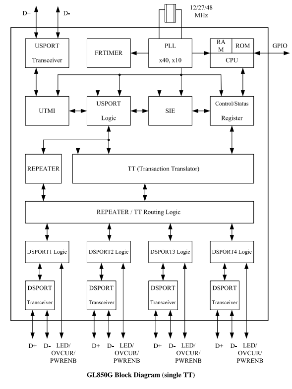
The GL850G functional block diagram shows how the USB hub controller manages communication between the host computer and multiple USB devices. At the top of the diagram, the upstream USB transceiver connects to the host through the D+ and D− lines. This section receives USB data from the computer and sends data back to the host. The built-in PLL uses an external 12/27/48 MHz clock source to generate stable internal timing signals required for USB communication.
Inside the controller, the CPU, RAM, ROM, SIE (Serial Interface Engine), and USB port logic work together to process USB packets, control hub functions, and manage data transfer. The CPU handles internal control operations, while the SIE processes USB protocol tasks such as packet decoding and device communication.
The Transaction Translator (TT) is one of the main blocks in the GL850G. It manages communication between high-speed USB 2.0 traffic and slower full-speed or low-speed USB devices connected to the downstream ports. Since the GL850G uses a single TT architecture, all downstream ports share the same translator logic.
At the bottom of the diagram, the repeater and downstream port logic distribute USB signals to multiple downstream USB ports. Each downstream port includes its own transceiver, power enable control, overcurrent detection, and LED status control signals for managing connected USB devices safely and reliably.
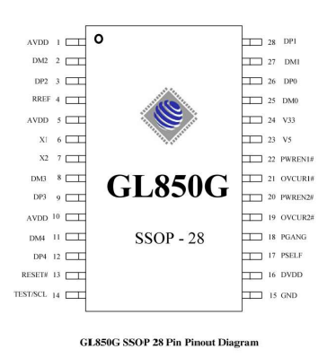
GL850G Pinout and Pin Functions
|
Pin
No. |
Pin
Name |
Pin
Function |
|
1 |
AVDD |
Analog power
supply input |
|
2 |
DM2 |
USB Port 2 D−
differential signal |
|
3 |
DP2 |
USB Port 2 D+
differential signal |
|
4 |
RREF |
Reference
resistor connection for internal circuit calibration |
|
5 |
AVDD |
Analog power
supply input |
|
6 |
X1 |
Crystal
oscillator or clock input |
|
7 |
X2 |
Crystal
oscillator output |
|
8 |
DM3 |
USB Port 3 D−
differential signal |
|
9 |
DP3 |
USB Port 3 D+
differential signal |
|
10 |
AVDD |
Analog power
supply input |
|
11 |
DM4 |
USB Port 4 D−
differential signal |
|
12 |
DP4 |
USB Port 4 D+
differential signal |
|
13 |
RESET# |
Active-low reset
input pin |
|
14 |
TEST/SCL |
Test mode pin or
SMBUS clock signal |
|
15 |
GND |
Ground
connection |
|
16 |
DVDD |
Digital power
supply input |
|
17 |
PSELF |
Self-powered
mode selection pin |
|
18 |
PGANG |
Gang power
management control pin |
|
19 |
OVCUR2# |
Overcurrent
detection input for Port 2 |
|
20 |
PWREN2# |
Power enable
output for Port 2 |
|
21 |
OVCUR1# |
Overcurrent
detection input for Port 1 |
|
22 |
PWREN1# |
Power enable
output for Port 1 |
|
23 |
V5 |
5V power input |
|
24 |
V33 |
Internal 3.3V
regulator output |
|
25 |
DM0 |
Upstream USB D−
differential signal |
|
26 |
DP0 |
Upstream USB D+
differential signal |
|
27 |
DM1 |
USB Port 1 D−
differential signal |
|
28 |
DP1 |
USB Port 1 D+
differential signal |
GL850G Typical Application Design
The GL850G typical application circuit shows how the hub controller is connected to the upstream USB port, downstream USB ports, clock source, power supply, and protection components. The GL850G acts as the main control IC that receives USB data from the host device through the upstream D+ and D− lines, then distributes the USB connection to multiple downstream USB ports.
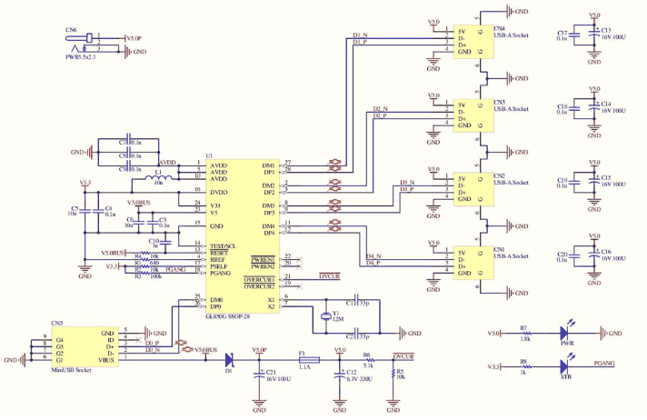
At the lower-left side of the circuit, the Mini USB connector is used as the upstream USB connection to the computer or host system. The upstream USB data lines connect directly to the GL850G upstream pins. A diode and fuse are added to help protect the circuit from reverse current and overcurrent conditions.
The crystal oscillator connected to the X1 and X2 pins provides the 12 MHz clock signal required for USB timing operation. Capacitors connected around the power pins help filter noise and stabilize the power supply for reliable USB communication.
On the right side of the circuit, the downstream USB ports are connected to the GL850G through separate D+ and D− signal lines. Each USB port also includes decoupling capacitors for power filtering. The PWREN and OVCUR pins are used for USB port power control and overcurrent detection, helping protect connected USB devices.
To use the GL850G, typically connect the upstream USB port, add a 12 MHz crystal, provide stable 5V power input, connect the downstream USB ports, and configure the power management pins properly. This allows the GL850G to function as a complete USB 2.0 hub controller with multiple downstream USB ports.
GL850G vs Other USB Hub Controllers
|
Feature |
GL850G |
GL852 |
FE1.1s |
USB
3.0 Hub Controllers |
|
USB Standard |
USB 2.0 |
USB 2.0 |
USB 2.0 |
USB 3.0 / USB
3.2 |
|
Maximum Speed |
480 Mbps |
480 Mbps |
480 Mbps |
5 Gbps or higher |
|
Transaction
Translator |
Single TT |
Multiple TT |
Single TT |
Multiple TT |
|
Performance With
Multiple USB Devices |
Moderate |
Better handling
of mixed-speed devices |
Basic
performance |
High-performance
multi-device support |
|
Cost |
Low |
Slightly higher
than GL850G |
Very low |
Higher |
|
Internal
Processor |
Built-in 8-bit
MCU |
Built-in MCU |
Simpler internal
architecture |
More advanced
controller architecture |
|
Power Management |
Individual and
gang mode support |
Advanced power
management |
Basic power
control |
Advanced smart
power management |
|
EEPROM / SMBUS
Support |
Yes |
Yes |
Limited |
Yes |
|
Best For |
Cost-effective
USB hubs |
Better USB 2.0
hub performance |
Simple low-cost
USB hubs |
High-speed
modern USB hubs |
|
Power
Consumption |
Low |
Low |
Very low |
Higher than USB
2.0 hubs |
|
Design
Complexity |
Moderate |
Moderate |
Simple |
More complex PCB
design |
|
Typical
Limitation |
Shared TT
bandwidth |
Higher cost |
Fewer advanced
features |
Higher cost and
power requirement |
Best Applications of GL850G
• USB 2.0 Hub Devices - Commonly used in multi-port USB hubs to expand one USB connection into several USB ports.
• Laptop Docking Stations - Helps add extra USB connectivity for keyboards, mice, flash drives, and printers.
• Embedded Systems - Used in embedded boards and industrial controllers that require multiple USB device connections.
• Industrial USB Expansion - Suitable for industrial equipment that needs stable USB communication with multiple peripherals.
• DIY USB Hub Projects - Popular among electronics hobbyists because of its low cost and relatively simple circuit design.
• Single Board Computer (SBC) Projects - Often integrated into Raspberry Pi and Linux-based systems for additional USB ports.
• USB Interface Modules - Used in systems that combine multiple USB devices into one compact board design.
• POS and Kiosk Systems - Helps connect barcode scanners, receipt printers, card readers, and other USB peripherals.
• Computer Monitor USB Hubs - Integrated inside monitors that provide built-in USB expansion ports.
• Low-Cost Consumer Electronics - Used in affordable USB accessories where USB 2.0 speed is sufficient for normal peripherals.
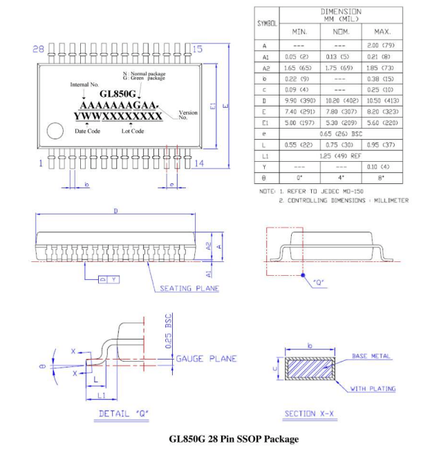
Mechanical Dimensions of GL850G
Manufacturer
Genesys Logic, the manufacturer of the GL850G, is a semiconductor company specializing in USB hub controllers, storage controllers, and interface IC solutions. The company supports large-scale IC manufacturing through advanced semiconductor design, packaging, testing, and quality control processes to ensure stable product performance and long-term reliability. Genesys Logic focuses on low-cost, highly integrated controller solutions that simplify PCB design and reduce BOM cost for manufacturers.
Frequently Asked Questions [FAQ]
1. Why does the GL850G use a Single Transaction Translator instead of Multiple Transaction Translators?
The GL850G uses a Single Transaction Translator (STT) mainly to reduce overall chip cost and simplify the hub architecture. In this design, all downstream full-speed and low-speed USB devices share the same transaction translator logic. This works well for normal USB peripherals like keyboards, mice, printers, and flash drives. However, if several slower USB devices transfer data heavily at the same time, bandwidth sharing may slightly reduce performance compared to multi-TT hub controllers.
2. How does the built-in 5V to 3.3V regulator help simplify USB hub design?
The integrated 5V to 3.3V regulator removes the need for a separate external regulator in many hub circuits. This helps reduce PCB space, lowers BOM cost, and simplifies power design. It also makes the overall USB hub circuit smaller and easier to manufacture.
3. Why is the 12 MHz crystal important in the GL850G circuit?
The 12 MHz crystal provides the reference clock needed for accurate USB timing. The built-in PLL multiplies this clock internally to generate stable timing signals for USB communication. Without accurate clock timing, USB data transfer can become unstable or fail completely.
4. What is the advantage of supporting both bus-powered and self-powered modes?
Supporting both modes gives designers more flexibility. Bus-powered mode allows the USB hub to operate directly from the host USB port, which is useful for compact low-power hubs. Self-powered mode uses an external power supply, allowing the hub to support higher-current USB devices more reliably.
5. How does the GL850G improve EMI performance in USB hub designs?
The GL850G includes slew-rate control in its output drivers to reduce sharp signal transitions on USB data lines. This helps lower electromagnetic interference (EMI), which improves signal stability and reduces the chance of communication problems caused by electrical noise.
6. Why are overcurrent detection and power enable pins important in USB hubs?
The OVCUR and PWREN pins help protect both the hub and connected USB devices. If a connected device draws too much current, the hub can detect the fault and disable power to the affected port. This improves safety and helps prevent hardware damage.
7. How does EEPROM support improve the flexibility of the GL850G?
EEPROM support allows manufacturers to customize VID, PID, downstream port settings, and power management behavior. This helps companies create branded USB hubs and configure the controller for different hardware designs without changing the main chip.
Verwandter Artikel
-
![Wichtiger Leitfaden für elektronische Smartwatch-Komponenten]() May 19 2026Wichtiger Leitfaden für elektronische Smartwatch-Komponenten
May 19 2026Wichtiger Leitfaden für elektronische Smartwatch-KomponentenIm Inneren einer Smartwatch befindet sich ein kompaktes System elektronischer Komponenten, die zusammenarbeiten.Wenn Sie diese Teile verstehen, verste...

Verwandte -Produkte
C1005X7R1C104M050BC
CAP CER 0.1UF 16V X7R 0402
CL10F105ZO8NNND
CAP CER 1UF 16V Y5V 0603
06033A6R0DAT2A
CAP CER 6PF 25V C0G/NP0 0603

ADS5413IPHP
IC ADC 11BIT PIPELINED 48HTQFP
MC100E446FN
IC INTERFACE SPECIALIZED 28PLCC

MAX9916EKA+T
IC OPAMP GP 2 CIRCUIT SOT23-8
MAX5351AEUA+T
IC DAC 13BIT V-OUT 8UMAX
LTC3862FE
LTC3862FE LINEAR
TM74HC245D
SOP20
UPD780076GK-710-ET-A
NEC QFP

TC74VHC4040AF
TC74VHC4040AF TOS

AM27C128-150BXA

S34ML01G200BHI0
SPANSION FBGA